The Evolution of Semiconductor Design
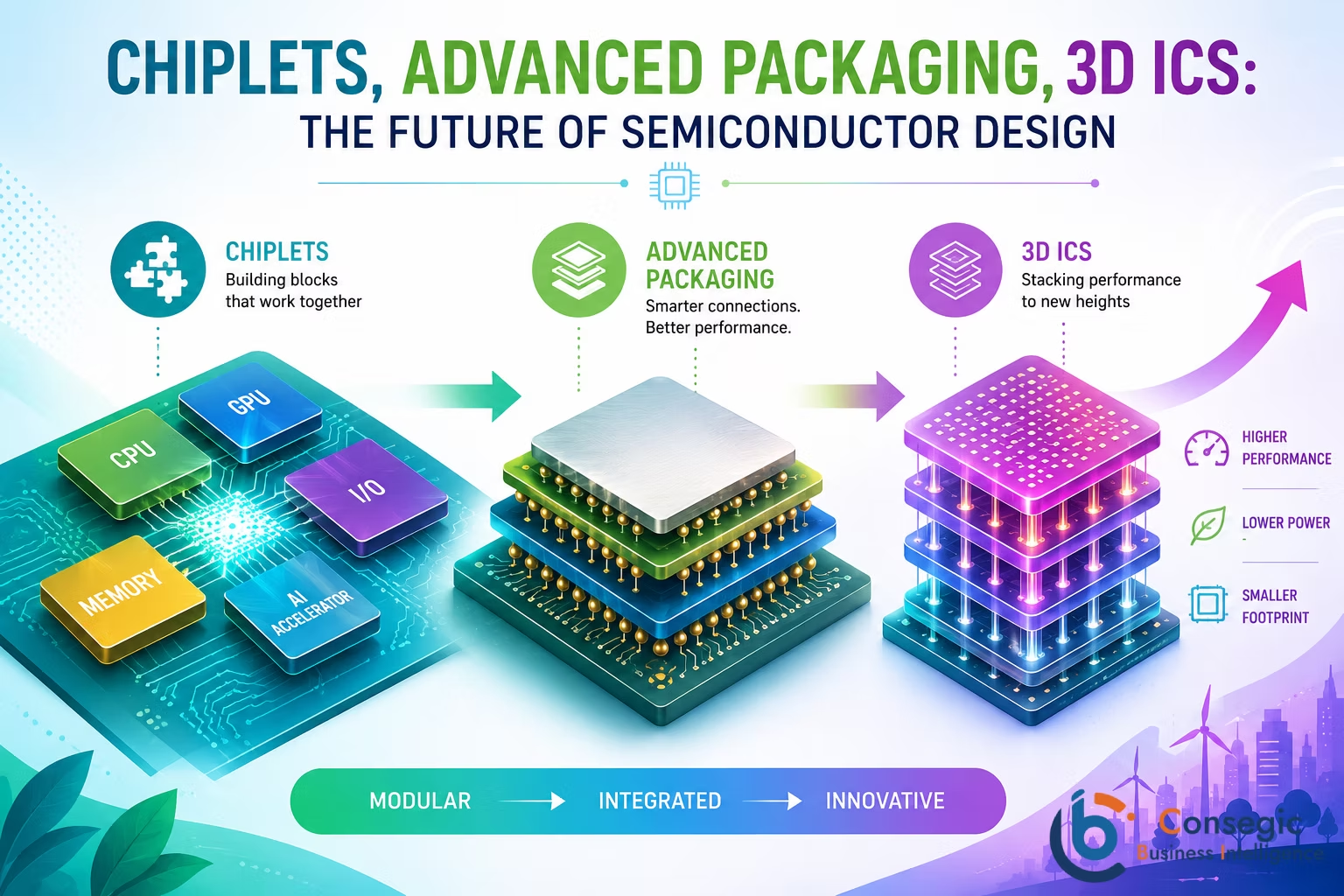
For many years, Moore's Law was used in the semiconductor industry to increase computing power by adding more transistors to smaller semiconductors. Nevertheless, due to increased cost and technological difficulties associated with further scaling of transistors, alternative methods have been considered that would help boost performance, increase efficiency and improve functionality of computer chips. Chiplets, advanced packaging, and 3D ICs are some of the key emerging technologies in this area. Unlike other technologies that focus on decreasing size of transistors to increase their number, the mentioned methods focus on integration, design and connection of particular components. The technology of chiplets allows decomposing complex processors into smaller components, advanced packaging technology – efficient communication between these components in one chip package, and 3D ICs technology – stacking semiconductor components to increase density and reduce distance between them. The mentioned technologies are going to change the paradigm of design and production of semiconductors. They will be especially valuable for such areas as artificial intelligence, high-performance computing, data centres, automotive electronics and advanced consumer devices.
Chiplets: Breaking Complex Chips into Smaller Building Blocks
One significant innovation that represents a considerable departure from monolithic chip manufacturing technology is the chiplet approach to system design. Herein, a complex system may be split into several smaller semiconductor components, which will perform particular functions. This means that a certain computing unit may consist of particular chiplets performing computing tasks, graphics operations, managing the memory of the device, as well as input/output tasks. The main advantage of the chiplet approach is the increased flexibility of design. In particular, companies can mix chiplets developed on various technological platforms thus using the most advanced manufacturing nodes where they are necessary. Additionally, the use of chiplets allows manufacturers to increase the yield of their products since smaller dies will contain fewer defects. Finally, a company can reuse particular designs of the chiplets in multiple product types. Thus, the development costs and time can be significantly reduced. However, systems based on chiplets will require highly effective interconnect standards and packaging solutions, as well as proper thermal management. With increasing demands for AI accelerators and performance processors, chiplets are becoming an attractive option to create such systems.
Advanced Packaging: Connecting Chips for Higher Performance
With traditional methods of enhancing the functionality of semiconductors being subject to physical and economic constraints, advanced packaging technology becomes an important tool in enhancing semiconductor efficiency. Rather than viewing semiconductor packaging as something that only provides protection for the chips inside the package, advanced semiconductor packaging technology brings about integration of numerous semiconductor components into a highly interconnected system. Through technologies such as 2.5D packaging, fan-out packaging, wafer-level packaging and high-bandwidth interconnects, processors, memory and chiplets can be enabled to communicate at high speeds without taking up a lot of space. Advanced semiconductor packaging technology has the ability to minimize the distance between components within the chip, hence helping increase bandwidth as well as increasing energy efficiency. It is especially useful when it comes to systems such as AI and high-performance computing since there is a lot of data transfer between processors and memory. Advanced packaging is increasingly becoming an integral part of system design through technologies such as silicon interposers and high bandwidth memory integration. However, advanced packaging is associated with certain challenges such as manufacturing challenges, thermal issues as well as high cost.
3D ICs: Building the Next Generation of High-Density Computing
Three-dimensional integrated circuits (3D IC) move the development of semiconductor integration a step ahead through the vertical stacking of several layers of circuitry. In contrast to conventional two-dimensional ICs in which components are mostly arranged horizontally next to each other, 3D IC allows for positioning dies or layers on top of each other. Electrical connection between those layers is enabled with the help of technologies like through-silicon vias (TSVs) and hybrid bonding. The use of 3D integration technology may significantly increase the density of transistors while decreasing the distance between processing and memory units. In such a way, 3D IC will ensure high bandwidth, performance and possibly less energy consumption. Memory solutions like 3D NAND have proven the benefits of vertical integration while applications in logic are being developed. 3D integration may also facilitate heterogenous architectures that will involve different technologies to be stacked according to their particular functions. Heat dissipation becomes one of the major problems since densely arranged layers make it harder to remove the generated heat. The problem of manufacturing complexity, yield, testing and reliability is also worth mentioning. Still, 3D ICs will definitely be used in future AI processors and HPC.
The Future of Semiconductor Design: Benefits, Challenges, and Industry Impact
The synergy between chiplets, advanced packaging, and 3D ICs gives birth to a new approach to semiconductor design. By no means can it be based on the sole reliance on the scaling of transistors; there is another way to enhance system performance through modular designs, advanced interconnections, and vertical integration. They can offer increased density of computation, higher bandwidth, improved energy efficiency, and flexibility. The innovations are especially relevant to artificial intelligence, cloud computing, autonomous driving, telecommunications and other fields that require high computing power. But there are a few hurdles to clear to take full advantage of these technologies. The manufacturing process gets more complicated; meanwhile, thermal management, testing, reliability, design requirements, and cost of production have to be considered. The industry needs to establish common standards of interoperability to ensure the successful integration of various chiplets produced by different vendors. Even so, semiconductor firms have already spent huge investments in the development of advanced packaging and heterogeneous integration. This suggests that the future of semiconductor design might be associated not with the creation of ever smaller single chip but with intelligent integration of technologies.
Conclusion
Chiplets, advanced packaging, and 3D ICs are revolutionizing semiconductor designs by offering innovative means to increase performance without wholly depending on conventional transistor scaling. These innovations offer increased levels of integration, fast communication, efficient energy usage, and system architecture flexibility. The use of such technologies in the field of artificial intelligence, high-performance computing, data centres, automotive electronics, and telecommunication is likely to increase with increased computer processing needs. There are challenges regarding issues of manufacture, heat management, testing, reliability, costs, and standardization that have to be addressed. With continuous investment in heterogeneous integration and advanced packaging, these technologies will gain prominence. In the end, the future of semiconductors lies in clever integration of small units, advanced packaging, and vertical integration.